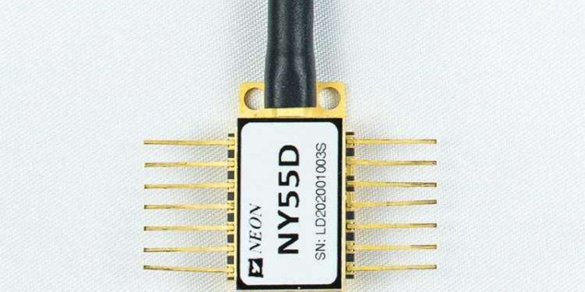
Photoconductive detector
The photoconductive detector is mainly detected by the change of the negative value. I will introduce its working principle by taking the photodiode as an example.
The photoresistor, also known as the light pipe, has no polarity and is purely a resistive device. It can be used with either a DC voltage or an AC voltage. When there is no light, the value of the photoresistor (dark resistance) is large, and the current (dark current) in the circuit is small. When the photoresistor is exposed to light in a certain wavelength range, its resistance (bright resistance) decreases sharply, and the current in the circuit increases rapidly.
Generally, it is hoped that the larger the dark resistance, the better, and the smaller the bright resistance, the better. At this time, the sensitivity of the photoresistor is high. The dark resistance value of the actual photoresistor is generally at the megohm level, and the bright resistance is below several thousand ohms.
Photovoltaic detector
Photovoltaic detectors are based on the principle of generating a potential difference from light and measuring the potential difference. It is divided into two types: photocells and photodiodes. Photocells are mainly devices that convert light energy into electrical energy. At present, there are selenium photocells, silicon photocells, gallium arsenide, germanium photocells, etc., but silicon photocells are currently the most widely used. Photodiodes are divided into P-N junction photodiodes, PIN photodiodes, avalanche photodiodes, photodiodes, etc.
Below I will introduce its working principle and its characteristics separately.
1) P-N junction photodiode
2) PIN photodiode is also known as a fast photodiode. Compared with ordinary photodiodes, it has a different time constant and makes the spectral response range shift to the long-wave direction, and its peak wavelength can be shifted to 1.04~1.06 um and corresponds to the emission wavelength of the YAG laser. It has the advantage of high sensitivity, so it is usually used for low-light detection (linear).
It is composed of a layer of intrinsic semiconductors sandwiched between a P-type semiconductor and an N-type semiconductor. Because the intrinsic semiconductor is similar to the medium, this is equivalent to increasing the distance between the two electrodes of the junction capacitance of the P-N junction, making the junction capacitance very small. Secondly, the width of the depletion layer in P-type semiconductors and N-type semiconductors widens with the increase of reverse voltage, and the junction capacitance also becomes small with the increase of reverse bias voltage.
Due to the existence of the I layer, and the P region is generally made very thin, the incident photons can only be absorbed in the I layer, and the reverse bias voltage is mainly concentrated in the I region, forming a high electric field region, and the photogenerated carriers in the I region are Under the action of a strong electric field, the motion is accelerated, so the carrier transit time constant is reduced, thereby improving the frequency response of the photodiode. At the same time, the introduction of the I layer enlarges the depletion region, broadens the effective working area of photoelectric conversion, and improves the sensitivity.


